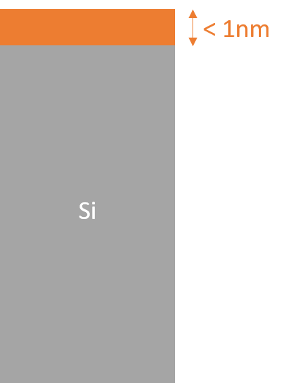
Which material can be used to protect a Si layer from Oxidation by a sub nanometer layer?
1 Answer
1nm layer is not much: let me remind you that this is roughly 10 atoms thickness...
But the good news is that we can easily create very thin films with a process of atomic layer deposition (ALD)
The isolating layer could be the classically grown $SiO_2$ (usually grown 0.5-2nm)
You could also use $TiO_2$ or $TiO_2/SiN_x$ stack which are also great for surface passivation but usually grown thicker 4-15nm
I would like to add that even if it will protect from a pure $O_2$ oxidation, at such dimensions the diffusivity of smaller particles is quite strong, the layer may also break from ions, and the layer will not be uniformly 1nm if the surface roughness is too important (will only work on properly polished Silicon wafer and not on the edges).
therefore in general we do not passivate (protection of aggressive elements) with such thin layer.
-
$\begingroup$ Nice answer ! Thank you very much. The Si would have to be carried in vacuum before the deposition in order to avoid natural Oxydation, right ?Do you know the ALD cycle for SiO2 ? I am wondering, if one is able to precisly deposit 0.5nm SiO2 ? $\endgroup$– jamesCommented Nov 23, 2017 at 16:39
-
$\begingroup$ consider that controlling a dielectric dep process to a thickness of five atoms means that to be "precise", you would have to deposit a layer not four atoms and not six atoms but 5 atoms thick: this would be impossible in practice. You might achieve this instead by exposing the Si to a chemical atmosphere in which it not only self-passivates but also self-limits the growth of the passivation, so as to make the process easier to control. Laying down exactly 5 atoms of anything, by any process, will be extremely hard to do consistently. $\endgroup$ Commented Nov 24, 2017 at 5:31
-
$\begingroup$ @Totyped in order to the three questions. 1) Wrong, oxidation is slow process enough in standard atm with no activator, dust is the main concern 2) can go down to some seconds per cycles but depends on tool, temp, ... 3) if your computer is recent, you should have there MOS devices with 0.5nm grown $SiO_2$ $\endgroup$– JonathanCommented Nov 24, 2017 at 14:43
-
$\begingroup$ @nielsnielsen ALD control is really good as it is a two step process, we really can grow atom layer per atom layer, so no issue for 5 atoms and not 4, but only if the initial surface is properly ready for welcoming these layer (ie perfect crystalline surface is required) most advanced devices uses such thickness, but for sure you won't afford to have this tool at home :P $\endgroup$– JonathanCommented Nov 24, 2017 at 14:52
-
$\begingroup$ @Jonathan Thank you very much for your answers ! This helps a lot ! :) $\endgroup$– jamesCommented Nov 24, 2017 at 19:15
